In-package optical I/O is the breakthrough technology needed to satisfy today’s computational workloads.
Today’s computational workloads are growing in both size and sophistication at an unprecedented rate. An emerging solution is to employ the composability capabilities provided by disaggregated architectures. However, the full potential of disaggregated architectures can be achieved only by means of state-of-the-art in-package optical input/output (I/O) technology.
Disaggregation and composability
A modern data center can contain tens or hundreds of thousands of cabinets or frames called racks. Each rack can contain anywhere from 10 to 40+ bays or shelves. In a traditional architecture, each shelf contains a server, and—in turn—each server features a motherboard containing one or more XPUs (CPUs, GPUs, FPGAs, ASICs, SoCs), memory in the form of DDR DRAM modules, and storage in the form of solid-state drives (SSDs).
Problems have emerged with this traditional architecture since computational workloads for tasks like AI and high-performance computing (HPC) have evolved to be larger, more complex, and more diverse than ever before. The solution is to use a disaggregated architecture, in which each shelf in the rack specializes in one type of component: CPUs, GPUs, RAMs, SSDs, etc. Using this form of disaggregated architecture leads to the concept of composability, in which virtualized resources are automatically composed in near real-time to meet the computational and memory requirements of each task on an application-specific basis. Once an application has completed its task, these resources are released back into their respective pools, at which point they can be provisioned to future applications in different ratios.
Introducing in-package optical I/O
For disaggregation and composability to work, it is necessary for data to be able to pass from shelf-to-shelf and rack-to-rack at lightning speed. Unfortunately, these bandwidth requirements far exceed the capabilities of traditional copper-based electrical interconnect technologies.
The solution is to use optical-based interconnect, but it is not sufficient to simply take existing devices (CPU, GPU, memory, etc.) and augment them with external optical interconnects. To achieve the necessary transmission speeds and bandwidths, it is required for the optical interconnect to be incorporated inside the device packages.
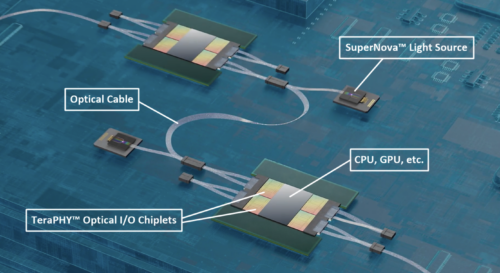
Fortunately, in-package optical I/O is now possible due to two recent developments from Ayar Labs in the form of TeraPHY optical I/O chiplets and SuperNova advanced light sources.
Chiplets are small integrated circuits, each containing a well-defined subset of functionality. Multiple chiplets can be combined with the main silicon die by means of a base layer called an interposer, with everything being presented as a single package to the outside world. By combining silicon photonics with standard CMOS manufacturing processes, TeraPHY optical I/O chiplets allow the core device to communicate with the outside world at the speed of light.
Each TeraPHY chiplet supports 2 terabits per second (Tbps) with a roadmap to 8Tbps. The remaining piece of the puzzle is provided by the SuperNova light source. The combination of TeraPHY chiplets and SuperNova light sources delivers up to 5X higher data rates with an 8X improvement in power efficiency compared to traditional copper-based electrical interconnect technologies. The Ayar Labs solution enables devices to communicate with each other across a wide range of distances, from millimeters to kilometers.
Almost unbelievably, it’s now possible for disaggregated racks of CPUs, GPUs, memory, and storage to be located tens, hundreds, or even thousands of meters from each other.