
Resets in FPGAs should be a first order consideration when planning and creating a design
by Rick Eggleton, Director of Learning Solutions at 2RTP
Resets in FPGAs are not as trivial as you may have been led to believe. Under the simple premise of returning the design to a known state resides a complex set of routes and delays that can make even the most seasoned designer cringe.
Due to fanout and other issues, resets tend to rapidly rise in complexity and, without a lot of careful planning and good methodologies, can be the most problematic issue a designer faces in design timing closure. Most of us were taught to “reset, reset, reset” and to “control, control, control.” This may be standard practice for ASIC design, but what about FPGAs?
Furthermore, there are the added complexities of Asynchronous versus Synchronous reset and Global versus a Local reset and, before long, your head starts to hurt. A good understanding of how to properly reset an FPGA is fundamentally required for a robust system.
Initially, no reset is better than having one (or more!). This does not mean that you should have no resets in your design, it simply means that you take care where and why resets are used. Most algorithms do not require a reset on every register, and some don’t require any resets at all. Unless there is a feedback path in an algorithm, all that really needs to be done is to let the data propagate to a known state. Data can then be enabled on the appropriate clock cycle. If the algorithm is processing unwanted data, that may not be a problem, simply ignore it. When you start introducing valid input data on the appropriate clock cycle, start collecting the propagated output. The invalid data passing through the system may be ignored. This is, most likely, the solution for the vast majority of a design.
For some parts of the design, a reset may be necessary. Resets are typically required when the design must be restored to a known starting point. Modules such as state machines, some control logic, and packet processing protocols that require specific execution order, are some examples of functions that require resets. However, before adding a reset to the design, ask two questions. Question 1: Does this signal really require a reset? If the answer is “No,” then don’t add a reset to that module. If the answer is “Yes,” then move on to Question 2: Does this signal really, really require a reset?
This forces a designer to evaluate the requirement more carefully. Rather than just assuming a reset is needed, consider the signal behavior, and then make the decision. Generally speaking, the majority of a design does not require a reset. If you’re unsure, don’t add the reset; instead, analyze the design further and figure it out. Adding unnecessary reset and control signals to a design can overburden the available routing resources or limit accessibility to certain resources.
If you add a global reset without carefully considering the consequences, you are most likely going to create insurmountable problems. The first thing to realize is that every AMD FPGA already has a global reset built in. When a bitstream is loaded, every register in the FPGA is initialized to either, ‘1’ or ‘0’. Unless the initialization state is specified in the design, the default is ‘0’.
The designer can specify the initialization state of every register as soon as the device becomes active following bitstream load. This is performed by initializing each register state in the HDL code. If a global reset is required, the register state should be specified as an initialization condition. Doing so eliminates the need for a second global reset.
To return to the initialization state, the GSR (Global Set/Reset) should be used. Instantiating the STARTUP block and toggling the GSR will reload the initialization condition into the device, thereby returning every register to its initial state… ergo, a global reset.
Using the GSR as the global reset does not consume any routing, nor does it require any specific timing constraints. By comparison, if a second global reset is added, it will be routed throughout the FPGA. This second global reset will span the entire design and will take a lot of careful planning, effort, and a few “tricks” (e.g., promoting the reset net to the global clock tree) to close timing.
This second global reset will have HUGE fanout and will consume a significant amount of routing resources. This net will also be one of the highest priorities for timing analysis and timing closure. The implementation tools will spend significant time and effort attempting to meet the constraints for the reset (notably each default clock period) and will typically fail. A global reset needs to pass timing analysis in every clock domain, otherwise the design will not function reliably.
Another consideration is whether to use asynchronous or synchronous resets. As stated earlier, no reset is best but—in an FPGA—synchronous resets are significantly better than their asynchronous counterparts. Static timing analysis (STA) tools are optimized for synchronous analysis. There is no way to analyze and guarantee error-free asynchronous behavior since, by definition, the relative timing between asynchronous signals is unknown.
Unless managed appropriately, asynchronous signaling results in metastability in a design. Metastability will, in most cases, lead to catastrophic results. Any asynchronous signal in an FPGA design should be synchronized immediately using correct clock domain crossing design techniques.
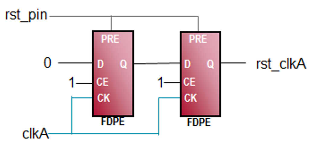
Individual signals may be managed using a “reset bridge” (pipelined flip-flops placed tightly together). A signal bus can be managed with a FIFO or other generally accepted techniques. However, even when using a FIFO, some individual signals must still be managed directly, for example, “full,” “almost full,” “empty,” and “almost empty,” Once these signals are synchronized to the local clock domains, the STA tools can work to close timing.
Resets in FPGAs should be a first order consideration when planning and creating a design. If a global reset is required, make sure you consider using the GSR rather than creating a high fanout, resource consuming, timing closure issue. Generally, most design modules and functions do not need to be reset; therefore, specific local resets are a much better solution. Last, but certainly not least, any asynchronous reset should be synchronized to the local clock domain first, otherwise metastability will occur.
If you’re looking for more information on resets—or any other aspect of FPGA and/or ASoC design or architecture—then feel free to contact us. Also, you will find a wide range of resources to satisfy your current needs or help prepare you for your next project on our website.